Publications
publications by categories in reversed chronological order.
Patents
-
More than 500 Patents Filed in US/Global/China.
Invited talks
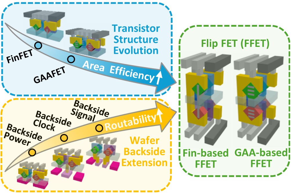
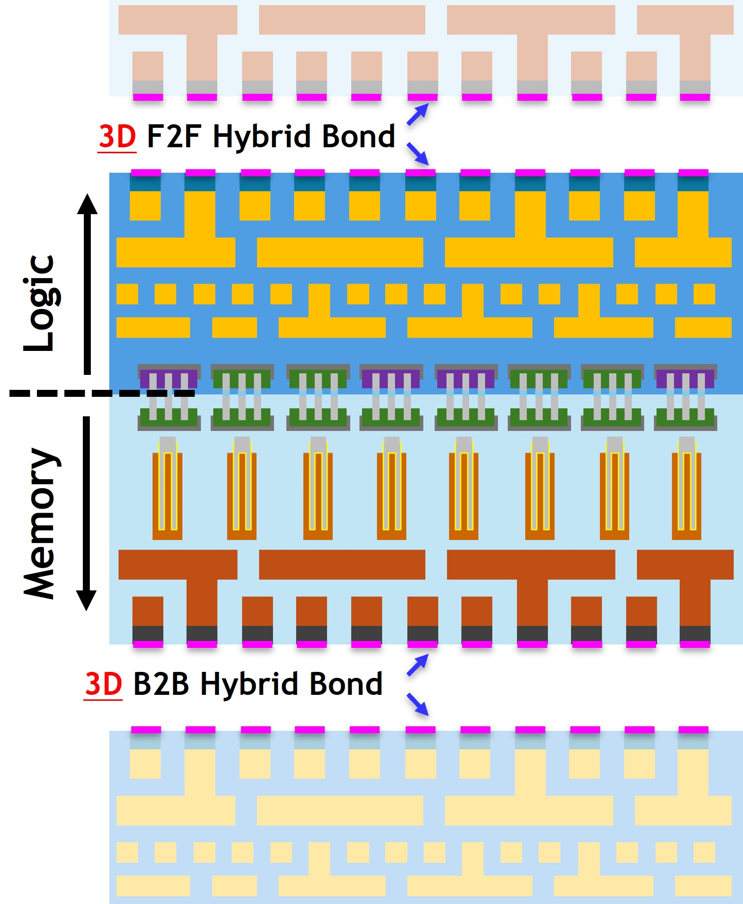
- H. Wu “Flip 3D (3D): A Novel 3D Integration for Multi-dimensional Stacking”, HiPi Annual Conference, Dec. 2025
- H. Wu “OPPORTUNITIES FOR ADVANCED LOGIC TECHNOLOGY WITH DUAL-SIDED INTEGRATIONS: FROM LATERAL TO VERTICAL TRANSISTORS “,2025 IEEE 16th International Conference on ASIC(ASICON), Kunming, China, Oct., 2025
- H. Wu “Flip 3D(F3D): A novel 3D Integration Technology Enabled by the Advanced Bonding”, International Workshop on Low Temperature Bonding for 3D Integration (LTB-3D), Tianjing, China, Aug., 2025
- H. Wu, “3D Integration Innovations and Opportunities on Both Sides of Wafer: A Design Perspective”, International Symposium of EDA 2025(ISEDA), Hong Kong SAR, China, May, 2025
- H. Wu, “Flip 3D (F3D) A dual-sided integration technology for future’s computing hardware”, 2025 CSTIC, Shanghai, China, Mar., 2025
- H. Wu, “From Flip FET to Flip 3D Integration (F3D): Maximizing the Scaling Potential of Wafer Both Sides Beyond Conventional 3D Integration”, The 9th IEEE Electron Devices Technology and Manufacturing Conference (EDTM),Hong Kong SAR, China, Mar., 2025
- H. Wu, “Flip 3D (F3D): A Novel Dual-Sided 3D Technology For Future”, 2024 National Vacuum and Semiconductor Technology Conference, Shanghai China, Nov., 2024
- H. Wu, “Flip 3D (F3D): A Novel 3D Integration Technology with Dual-side Integration Capabilities”, IEEE ICSICT, Zhuhai, China, Oct., 2024
- H. Wu, “Flip 3D Integration:” Flip 3D Integration: A Novel 3D Integration Technology with Dual-side Active and Interconnects Beyond CFET and BSPDN”, The 19th National Semiconductor and Integrated Technology Conference, Nanjing, China, Aug., 2024
- H. Wu, “Logic M3D For Future Giving Ge a Second Opportunity”, Semiconductor Technology Forum, Beijing, China, Nov., 2023
- H. Wu, “Consideration of Logic Technology for GAA and Beyond in Angstrom Age”, STW, Shenzheng, China, Sep., 2023
- H. Wu, “Low Temperature Ge CMOS for Future M3D Technology”, 2023 CSTIC, Shanghai, China, July, 2023
- H. Wu, “Logic M3D For Future Giving Ge a Second Chance”, National Semiconductor Physics Conference, Shanghai, China, July, 2023
- H. Wu and P. D. Ye, “Ge CMOS Devices and Logic Circuits”, International Conference on Solid State Devices and Materials (SSDM), Sapporo, Japan, September 2015.
Conference and Journal Papers
2026
-
 A Noval Dual-sided Method for Precise Resistance and Capacitance Partition in GAA Transistors with Backside ContactsIn IEEE Transactions on Electron Devices , 2026
2025
- IEDM
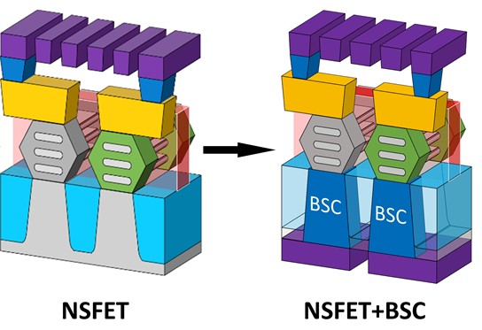
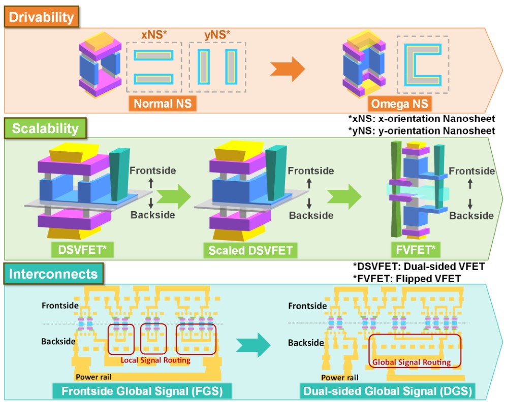 Extending Vertical FET for Advanced Logic Scaling with Architecture Innovations: Dual-sided Global Signal, Flip VFET and Omega NanosheetIn 2025 IEEE International Electron Devices Meeting(IEDM), 2025
 - IEDMHigh-Density RRAM for Advanced Logic Process: A Hybrid-Driven Cell with Self-Aligned Isolation Scalable to FinFET TechnologyIn 2025 IEEE International Electron Devices Meeting(IEDM), 2025
- Vertical Channel Gate-all-around(VCG) CMOS Transistors with MBE in-situ Doping Channel and TiN/HfO2 Gate StacksIn 2025 Electron Devices Technology and Manufacturing Conference (EDTM), 2025
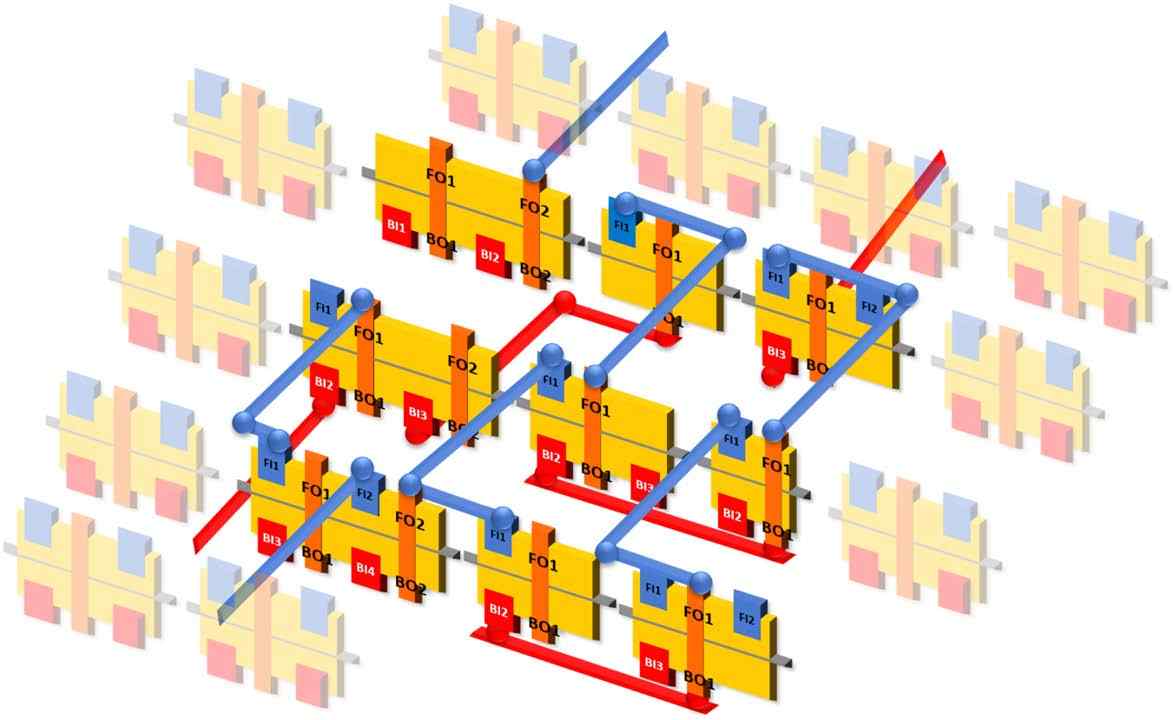
- A Systematic Approach for Multi-Objective Double-Side Clock Tree SynthesisIn 2025 ACM/IEEE Design Automation Conference (DAC), 2025
- Low Thermal Budget Ultrathin Ti Silicide for Advanced Backside Contact of Backside Power Delivery Network (BSPDN)In 2025 Electron Devices Technology and Manufacturing Conference (EDTM), 2025
- Overlay-Aware Variation Study of Flip FET and Benchmark with CFETIn 2025 Electron Devices Technology and Manufacturing Conference (EDTM), 2025
- Consideration of VFET for Ultimate Logic Scaling: A Design PerspectiveIn 2025 Electron Devices Technology and Manufacturing Conference (EDTM), 2025
- Performance Enhancement Strategies in Vertical FETs for Next-Generation LogicsIn 2025 International Conference on Solid State Devices and Materials (SSDM), 2025
-
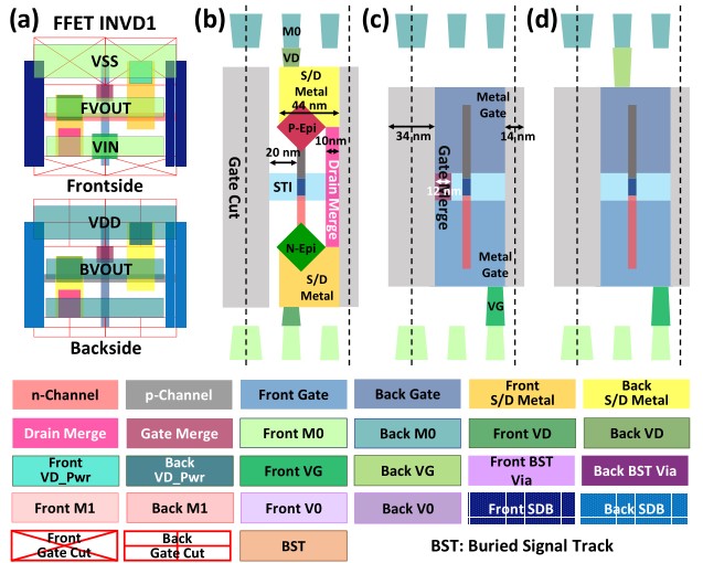
 A Tale of Two Sides of Wafer: Physical Implementation and Block-Level PPA on Flip FET with Dual-sided SignalsIn 2025 Design, Automation and Test in Europe Conference (DATE), 2025
 - Stacked Transistors with Nanosheet-based Flip FET for A10 Node: A DTCO ViewpointIn 2025 International Conference on Solid State Devices and Materials (SSDM), 2025
-
 Design Optimization of Flip FET Standard Cells with Dual-sided Pins for Ultimate ScalingIEEE Transactions on Electron Devices, 2025
 - Self-limited Ti Silicide Contact at 350°C for Dual-Side Wafer-Level IntegrationIEEE Electron Device Letters, 2025
-
 Understanding of the Electrostatic Coupling in Flip FET (FFET) and Corresponding StrategiesIEEE Transactions on Electron Devices, 2025
 -
 Stress-Aware Performance Optimization in Gate-All-Around NSFET and BeyondIEEE Transactions on Electron Devices, 2025
2024
- Modeling the Parasitic Resistances and Capacitances of Advanced Vertical Gate-All-Around TransistorsIEEE Transactions on Electron Devices, 2024
- Understanding of Channel Profile Impact of Fin-based Flip-FETIn IEEE Semiconductor Interface Specialists Conference, 2024

2022
- Scatterometry-based methodologies for characterization of MRAM technologyIn Metrology, Inspection, and Process Control XXXVI, 2022
2021
- IEDM
 First experimental demonstration of MRAM data scrubbing: 80 Mb MRAM with 40 nm junctions for last level cache applicationsIn 2021 IEEE International Electron Devices Meeting (IEDM), 2021
 - IEDM
 Vertical-transport nanosheet technology for CMOS scaling beyond lateral-transport devicesIn 2021 IEEE International Electron Devices Meeting (IEDM), 2021
2020
- VLSI
 Improved air spacer co-integrated with self-aligned contact (SAC) and contact over active gate (COAG) for highly scaled CMOS technologyIn 2020 IEEE Symposium on VLSI Technology(VLSI), 2020
 - IEDM
 A 14 nm embedded stt-mram cmos technologyIn 2020 IEEE International Electron Devices Meeting (IEDM), 2020
 - Improved air spacer for highly scaled CMOS technologyIEEE Transactions on Electron Devices, 2020
- Parasitic resistance reduction for aggressively scaled stacked nanosheet transistorsIn 2020 IEEE International Interconnect Technology Conference (IITC), 2020
2019
- VLSI
 Direct Partition Measurement of Parasitic Resistance Components in Advanced Transistor ArchitecturesIn 2019 Symposium on VLSI Technology(VLSI), 2019
 - IEDM
 Full bottom dielectric isolation to enable stacked nanosheet transistor for low power and high performance applicationsIn 2019 IEEE International Electron Devices Meeting (IEDM), 2019
 - Experimental extraction of ballisticity in germanium nanowire nMOSFETsIEEE Transactions on Electron Devices, 2019
2018
- VLSI
 Leakage aware Si/SiGe CMOS FinFET for low power applicationsIn 2018 IEEE Symposium on VLSI Technology(VLSI), 2018
 - IEDM
 External resistance reduction by nanosecond laser anneal in Si/SiGe CMOS technologyIn 2018 IEEE International Electron Devices Meeting (IEDM), 2018
 - IEDM
 Parasitic resistance reduction strategies for advanced CMOS FinFETs beyond 7nmIn 2018 IEEE International Electron Devices Meeting (IEDM), 2018
 - Performance potential of Ge CMOS technology from a material-device-circuit perspectiveIEEE Transactions on Electron Devices, 2018
- Mobility fluctuation-induced low-frequency noise in ultrascaled Ge nanowire nMOSFETs with near-ballistic transportIEEE Transactions on Electron Devices, 2018
- Integration of Germanium into Modern CMOS: Challenges and BreakthroughsAdvanced Nanoelectronics: Post-Silicon Materials and Devices, 2018
- Contact metallization for advanced CMOS technology nodesIn 2018 IEEE International Interconnect Technology Conference (IITC), 2018
2017
- IEDM
 Integrated dual SPE processes with low contact resistivity for future CMOS technologiesIn 2017 IEEE International Electron Devices Meeting (IEDM), 2017
 - Experimental Investigation of Ballistic Carrier Transport for Sub-100 nm Ge n-MOSFETsIEEE Electron Device Letters, 2017
- Anomalous bias temperature instability on accumulation-mode Ge and III-V MOSFETsIn 2017 IEEE International Reliability Physics Symposium (IRPS), 2017
- Carrier mobility enhancement by applying back-gate bias in Ge-on-insulator MOSFETsIEEE Electron Device Letters, 2017
- Development of TiO2 containing hardmasks through PEALD depositionIn Advances in Patterning Materials and Processes XXXIV, 2017
-
2016
- VLSI
 RTN and low frequency noise on ultra-scaled near-ballistic Ge nanowire nMOSFETsIn 2016 IEEE Symposium on VLSI Technology(VLSI), 2016
 - IEDM
 Substrate and layout engineering to suppress self-heating in floating body transistorsIn Electron Devices Meeting (IEDM), 2016 IEEE International, 2016
 - High-performance InAlN/GaN MOSHEMTs enabled by atomic layer epitaxy MgCaO as gate dielectricIEEE Electron Device Letters, 2016
- Gate length dependence of bias temperature instability behavior in short channel SOI MOSFETsMicroelectronics Reliability, 2016
- Demonstration of Ge Nanowire CMOS Devices and Circuits for Ultimate ScalingIEEE Transactions on Electron Devices, 2016
- Fully Depleted Ge CMOS Devices and Logic Circuits on SiIEEE Transactions on Electron Devices, 2016
- Total Ionizing Dose (TID) Effects in Ultra-Thin Body Ge on Insulator (GOI) Junctionless CMOSFETs with Recessed Source/Drain and ChannelIn IEEE Nuclear and Space Radiation Effects Conference, 2016
- Modeling of GeOI and Validation with Ge-CMOS Inverter Circuit using BSIM-IMG Industry Standard ModelIn IEEE International Conference on Electron Devices and Solid-State Circuits, 2016
2015
- VLSI
 First experimental demonstration of Ge 3D FinFET CMOS circuitsIn 2015 Symposium on VLSI Technology (VLSI Technology), 2015
 - IEDM
 First demonstration of Ge nanowire CMOS circuits: Lowest SS of 64 mV/dec, highest gmax of 1057 uS/um in Ge nFETs and highest maximum voltage gain of 54 V/V in Ge CMOS invertersIn 2015 IEEE International Electron Devices Meeting (IEDM), 2015
 - Inversion-mode GaAs wave-shaped field-effect transistor on GaAs (100) substrateApplied Physics Letters, 2015
- Germanium nMOSFETs with recessed channel and S/D: Contact, scalability, interface, and drain current exceeding 1 A/mmIEEE Transactions on Electron Devices, 2015
- Demonstration of Ge CMOS inverter and ring oscillator with 10 nm ultra-thin channelIn 2015 73rd Annual Device Research Conference (DRC), 2015
- Ge CMOS Devices: Performance and Variation Dependence on Operation Mode and Channel ThicknessIn IEEE Semiconductor Interface Specialists Conference, 2015
-
- Ge CMOS Devices and Logic CircuitsIn International Conference on Solid State Devices and Materials, 2015
- Back Gate Bias induced Carrier Mobility Enhancement in Ge-on-insulator MOSFETsIn IEEE Semiconductor Interface Specialists Conference, 2015
- InAlN/GaN MOSHEMTs with High Drain Current of 2.3 A/mm High On/Off Ratio of 1012 and low SS of 64 mV/dec Enabled by Atomic-Layer-Epitaxial MgCaO as Gate DielectricIn 2015 73rd Annual Device Research Conference (DRC), 2015
2014
- VLSI
 Ge CMOS: Breakthroughs of nFETs (I max= 714 mA/mm, g max= 590 mS/mm) by recessed channel and S/DIn 2014 Symposium on VLSI Technology (VLSI-Technology), 2014
 - VLSI
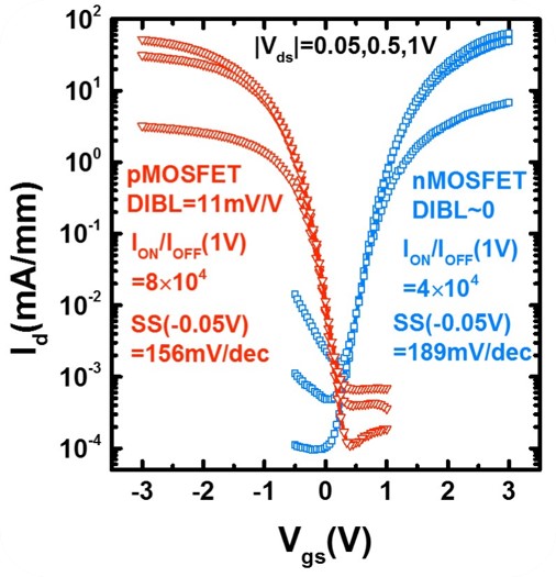
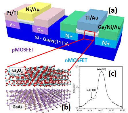 III-V CMOS devices and circuits with high-quality atomic-layer-epitaxial La 2 O 3/GaAs interfaceIn 2014 Symposium on VLSI technology (VLSI-Technology): digest of technical papers, 2014
 - VLSI
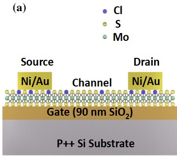 High-performance MoS2 field-effect transistors enabled by chloride doping: Record low contact resistance (0.5 Kohm*um2) and record high drain current (460 uA/um)In 2014 Symposium on VLSI Technology (VLSI-Technology), 2014
 - IEDM
 Deep sub-100 nm Ge CMOS devices on Si with the recessed S/D and channelIn 2014 IEEE International Electron Devices Meeting(IEDM), 2014
 - IEDM
 First experimental demonstration of Ge CMOS circuitsIn 2014 IEEE International Electron Devices Meeting(IEDM), 2014
 - Chloride molecular doping technique on 2D materials: WS2 and MoS2Nano letters, 2014
- InAs gate-all-around nanowire MOSFETs by top-down approachIn 72nd Device Research Conference, 2014
- Ge nFETs: A Study on Interface and Contact ResistanceIn IEEE Semiconductor Interface Specialists Conference, 2014
2013
- Room-temperature quantum oscillations in Ge junctionless MOSFETs at the scaling limitIn 71st Device Research Conference, 2013
- Performance enhancement of gate-all-around InGaAs nanowire MOSFETs by raised source and drain structureIn 71st Device Research Conference, 2013
- Variability improvement by interface passivation and EOT scaling of InGaAs nanowire MOSFETsIEEE Electron Device Letters, 2013
- Performance and variability studies of InGaAs gate-all-around nanowire MOSFETsIEEE Transactions on Device and Materials Reliability, 2013
- Ultra-scaled Junctionless MOSFETs on GeOI SubstratesIn IEEE Semiconductor Interface Specialists Conference, 2013
- Ultimately Scaled Sub-10nm V-Gate InGaAs MOSFETsIn IEEE Semiconductor Interface Specialists Conference, 2013
2012
- Size-Dependent-Transport Study of In0.53Ga0.47As Gate-All-Around Nanowire MOSFETs: Impact of Quantum Confinement and Volume InversionIEEE electron device letters, 2012
- IEDM
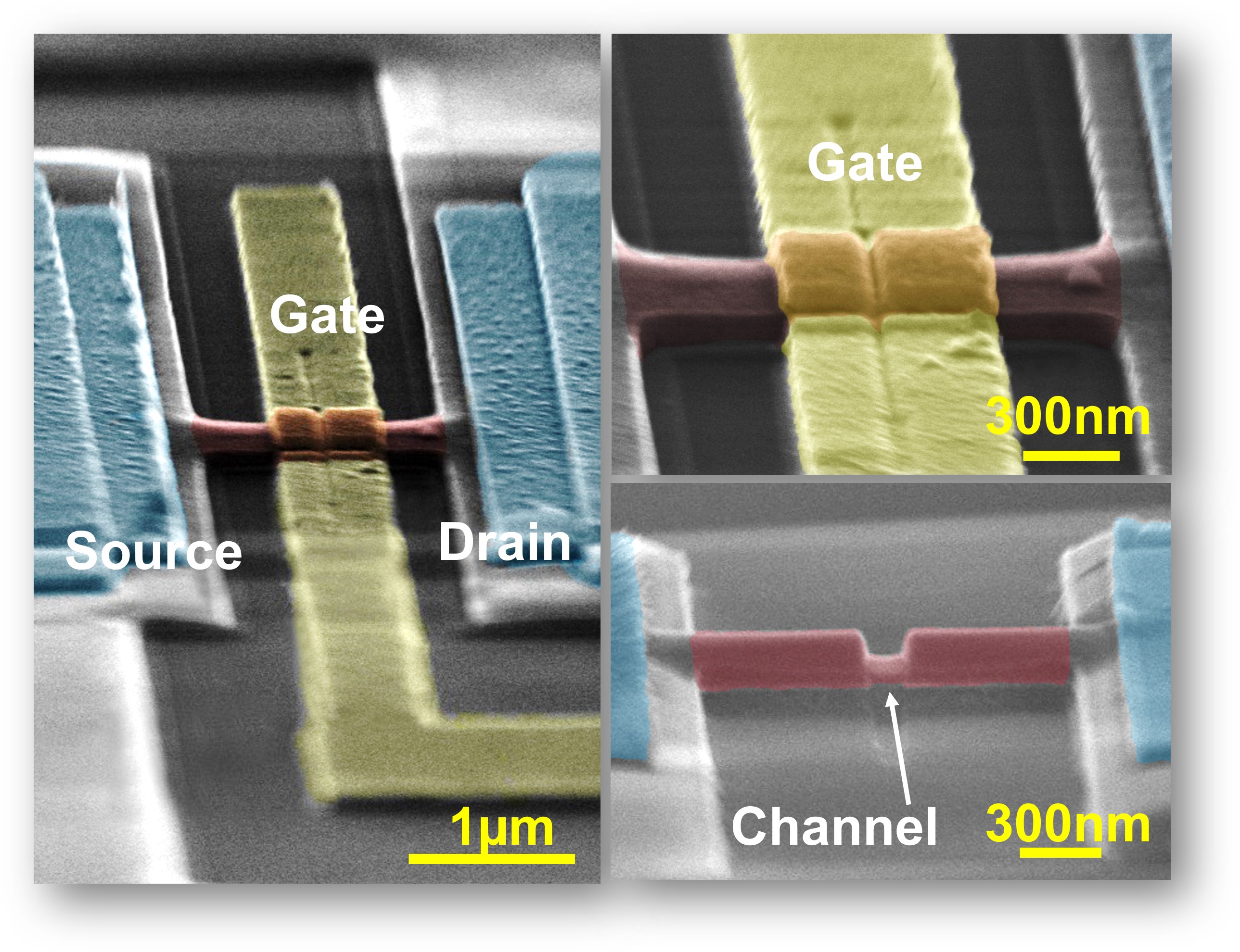
 20–80nm Channel length InGaAs gate-all-around nanowire MOSFETs with EOT= 1.2 nm and lowest SS= 63mV/decIn 2012 International Electron Devices Meeting(IEDM), 2012
 - In-situ SRPES study on the band alignment of (0001) CdS/CdTe heterojunctionChinese Physics Letters, 2012