Dualside Design
The circuit design innovations for both sides of wafer
Circuit Design Innovations for Dual-Sided Circuits on Wafer are crucial for the next generation of semiconductor devices. As the demand for smaller, faster, and more energy-efficient electronics grows, dual-sided circuits—where both the front and back sides of a wafer are used for circuit integration—offer a promising solution. This approach enables higher transistor density, reduced power consumption, and improved performance by utilizing the full potential of the wafer space.
To make dual-sided circuits a reality, several innovations in circuit design are required. These include advanced 3D integration techniques, precise alignment methods, and novel interconnect strategies that can connect the front and back sides efficiently. Additionally, new materials and packaging technologies are needed to support high-speed data transfer and heat management in these compact, high-density designs.
These innovations will be key to developing future electronics that power everything from mobile devices to data centers, enabling continued progress in semiconductor miniaturization and performance.

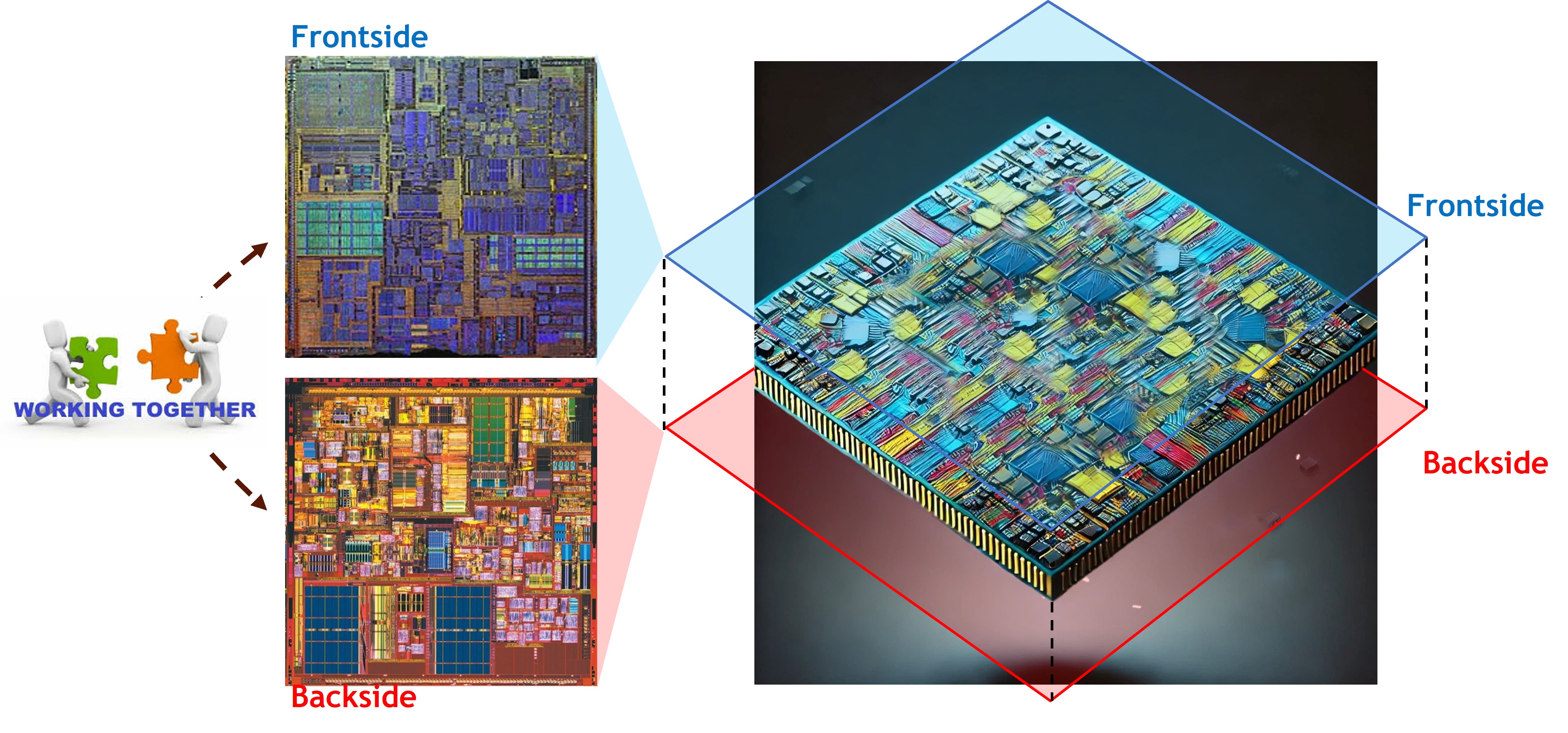
Above showcases both the frontside and backside of a semiconductor wafer. This approach involves utilizing both sides of the wafer for circuit integration, allowing for denser, more efficient designs that optimize the use of available space.
Key innovations in dual-sided circuit design include:
-
Frontside and Backside Integration: The image highlights how both sides of the wafer are used to integrate circuits, with each side designed to complement the other. This requires precise alignment and advanced bonding techniques to ensure that both sides work together seamlessly.
-
Advanced Layering Techniques: To achieve higher functionality in smaller form factors, new layering technologies are essential. This includes innovative deposition and etching techniques to create high-performance circuits on both sides of the wafer.
-
Interconnects for Dual-Sided Integration: Innovations in interconnect technologies are crucial for linking the front and backside circuits. This may involve advanced super vias (SV) or vertical interconnects to provide efficient electrical connections between the two sides.
-
Thermal Management: Managing heat in dual-sided circuits is essential due to the increased density and the need for efficient cooling. Thermal innovations in packaging and heat dissipation must be incorporated to maintain device reliability and performance.
These innovations enable more compact, faster, and more power-efficient devices, supporting the development of next-generation electronics. The dual-sided circuit design methodology is key to advancing semiconductor technology, especially as the demand for higher performance and miniaturization grows.

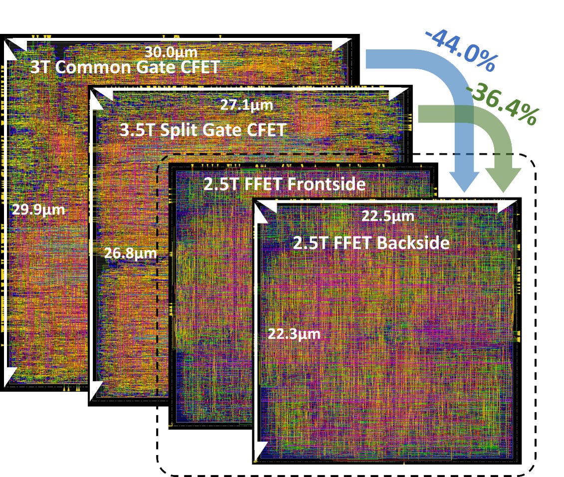
Above showcases various dual-sided Place and Route (PnR) designs, highlighting innovations required in Electronic Design Automation (EDA) for optimizing layout and routing in circuits that utilize both the frontside and backside of the wafer.
Here are the key points focused on EDA innovations for dual-sided Place and Route:
-
Integration of Front and Backside Layers: The image compares different designs, including 3T Common Gate CFET, 3.5T Split Gate CFET, and 2.5T FFET on both the front and backside of the wafer. EDA tools must efficiently manage the complex task of integrating circuits on both sides, requiring innovations in layer-aware routing algorithms that ensure seamless connections across the front and back.
-
Reduced Footprint and Optimization: As shown, the backside circuit design has a smaller footprint (22.5 µm) compared to traditional designs (29.9 µm for 3T Common Gate CFET). EDA innovations allow for space-saving techniques by optimizing interconnects and routing paths, leading to higher density designs with reduced chip area, while also maintaining electrical performance.
-
Advanced Routing for Reduced Power Consumption: The image displays how advanced routing algorithms and power grid optimizations can significantly reduce the area occupied by transistors and interconnects (e.g., the 2.5T FFET Frontside and Backside design reduces area by up to 44% and 36.4%, respectively). These EDA innovations help in achieving power-efficient designs, balancing the demand for high performance with low power consumption.
-
Cross-Layer Connectivity: Dual-sided design requires innovative interconnect technologies, such as through-silicon vias (TSVs) and vertical interconnects, to connect circuits across the front and backside layers. EDA tools need to account for these vertical connections during the place and route process, ensuring that signal integrity and timing constraints are met.
In summary, these EDA innovations enable the development of dual-sided Place and Route solutions that optimize space, reduce power consumption, and ensure the efficient integration of front and backside circuits, paving the way for next-generation high-density semiconductor devices.