Novel Device
Innovative Device to Drive IC further
Transistor Stacking beyond GAA represents the next frontier in semiconductor innovation, aiming to push the limits of device scaling and performance. While Gate-All-Around (GAA) transistors have enabled significant improvements in miniaturization and efficiency, stacking technologies extend these advancements by vertically stacking multiple transistor layers. This approach offers several advantages, including enhanced drive current, reduced footprint, and increased transistor density, all while maintaining low power consumption.
The key benefit of transistor stacking is the ability to integrate multiple logic and memory layers in a single package, addressing the growing demand for high-performance computing, memory-intensive applications, and miniaturized devices. By utilizing 3D stacking, these technologies enable the development of chips that are more powerful and efficient, which are crucial for the next generation of mobile, AI, and data center applications.
With continued advancements in material science, bonding techniques, and fabrication processes, transistor stacking beyond GAA holds the potential to enable even smaller, faster, and more energy-efficient devices, driving the future of integrated circuit design.

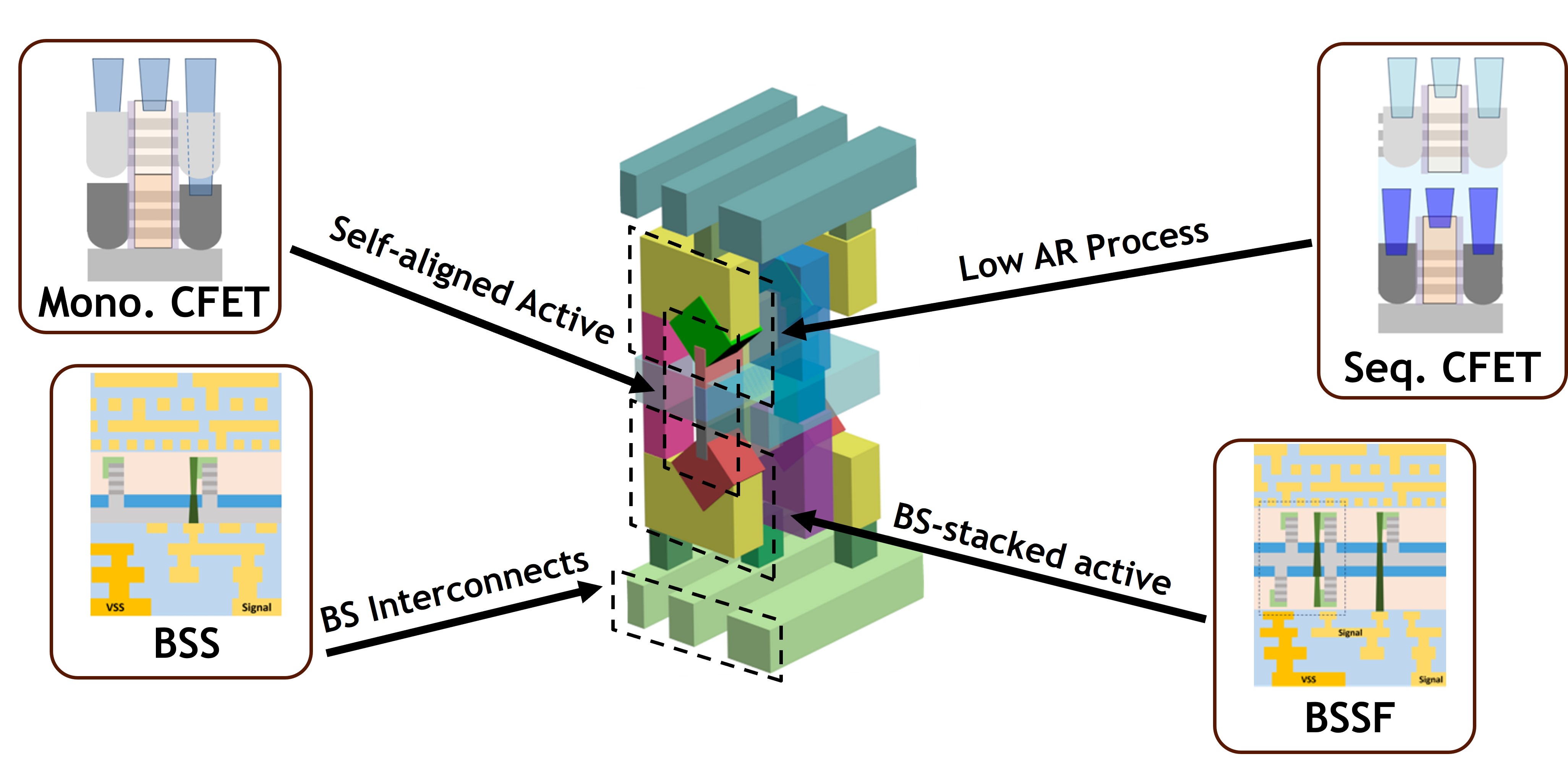
The figure showcases several device architecture innovations focused on next-generation semiconductor technologies. These innovations aim to enhance the performance and scalability of transistor and interconnect designs.
-
Mono. CFET (Monolithic CFET): The architecture features a self-aligned active region, improving device alignment precision and reducing process complexity. This structure allows for better integration of complementary devices in a monolithic configuration, enhancing performance without sacrificing chip area.
-
Seq. CFET (Sequential CFET): This sequential configuration focuses on stacking complementary transistors with optimized interconnections. The Low AR (Aspect Ratio) Process enables efficient stacking of the devices while maintaining excellent electrical properties. This architecture is designed to meet the growing demand for higher device density and performance.
-
BSS (Backside Signal): The BSS structure integrates backside interconnects with advanced BS Interconnects, enabling more efficient signal transmission and reducing the footprint of the overall chip. This architecture is especially useful for improving power delivery and thermal management in dense designs.
-
BSSF (Backside Stacked FET): This configuration integrates backside interconnects and self-aligned active regions. It improves signal integrity and provides a compact form factor, which is critical for high-performance applications, such as advanced logic and memory integration.
Together, these architectural innovations represent cutting-edge approaches to overcoming the challenges of transistor scaling, providing enhanced electrical performance, and optimizing chip design for the next generation of high-density, high-performance systems.

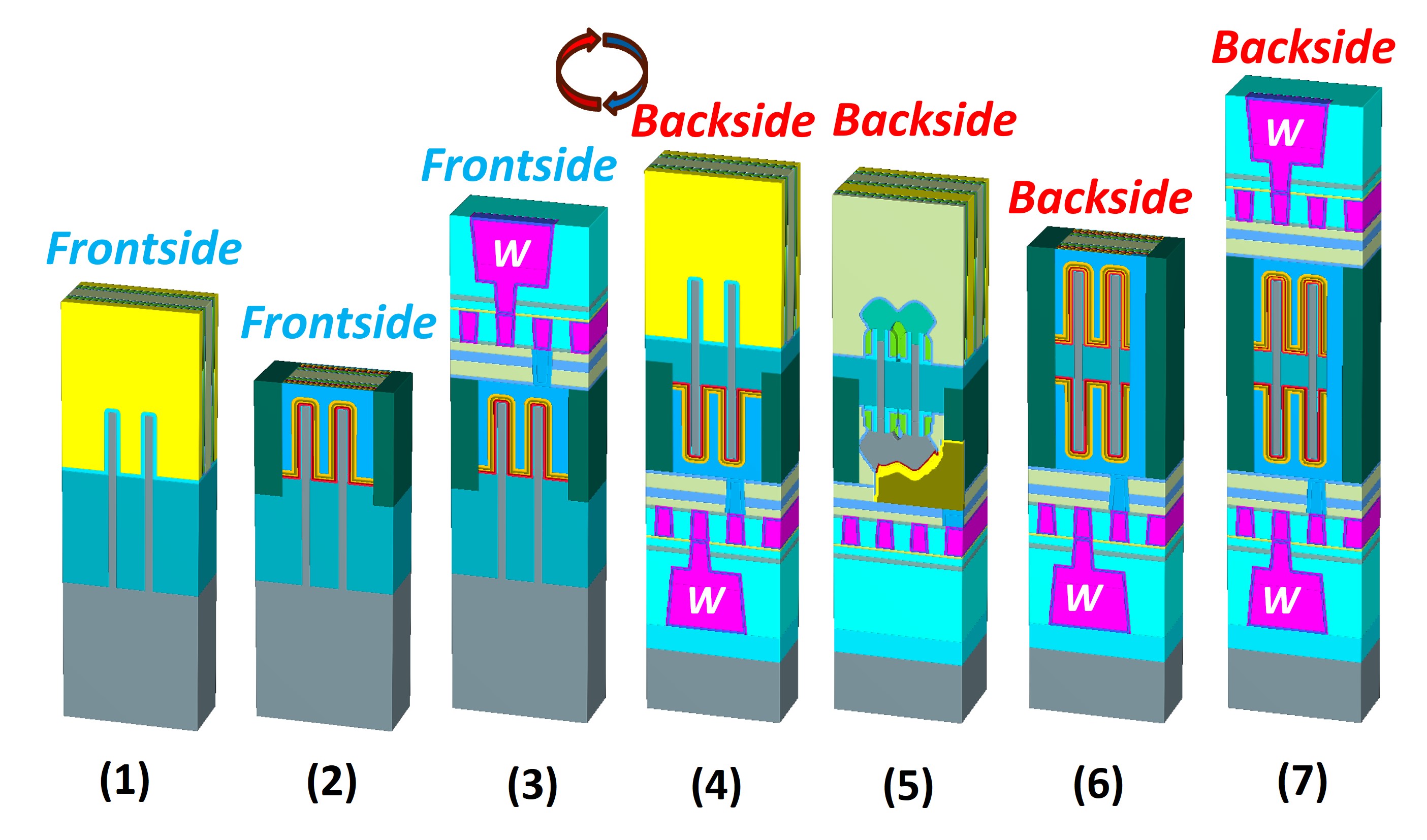
The figure outlines the Flip FET process flow, which includes key innovations necessary for its development:
- Frontside Processing: Involves patterning and depositing key layers, requiring precision in material deposition and patterning techniques.
- Frontside Layering and Interconnects: Focuses on creating interconnections with innovations in low-resistance materials and fine-pitch techniques.
- Backside Processing: Introduces challenges in wafer thinning and backside alignment, essential for achieving the 3D Flip FET structure.
- Backside Layering and Interconnects: Requires advanced bonding and stacking techniques, ensuring robust connections and maintaining performance.
These stages highlight the need for innovations in 3D integration, wafer thinning, and precise bonding to create high-performance, compact Flip FET devices.