3D Integration
3D integration enables the scaling beyond Moore's Law
3D Integration for CMOS Logic Technology is an advanced semiconductor packaging technique that enables the stacking of multiple layers of integrated circuits (ICs) vertically. This approach significantly enhances the performance and functionality of CMOS (Complementary Metal-Oxide-Semiconductor) logic devices while reducing the footprint and power consumption. By stacking chips in a 3D configuration, the distance between components is minimized, allowing for faster signal transmission and improved bandwidth.
This technology is particularly beneficial in addressing the challenges of Moore’s Law, enabling the continued miniaturization of devices without compromising performance. 3D integration also facilitates the integration of heterogeneous components, such as memory and logic, within a single package, enabling new applications in high-performance computing, mobile devices, and IoT systems. As the demand for faster, smaller, and more energy-efficient electronics continues to grow, 3D Integration is poised to play a crucial role in the future of CMOS logic technology.

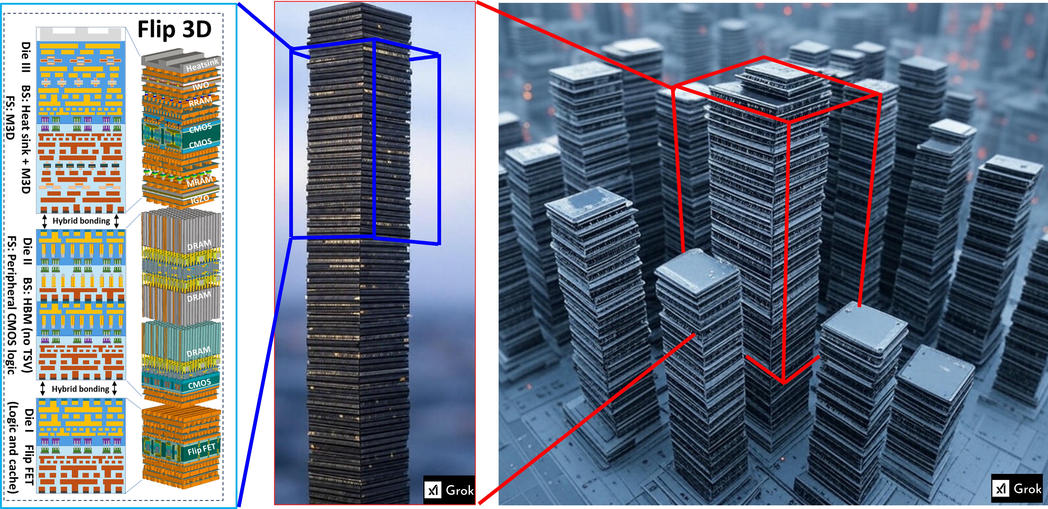
The figure showcases 3D Integration for CMOS logic technology with a focus on a stacked die architecture for advanced semiconductor systems. It visually represents the process of vertically stacking multiple layers of integrated circuits (ICs) to form a 3D package, a technique commonly used to enhance performance and reduce the footprint of devices.
On the left side, a diagram shows a cross-sectional view of multiple stacked dies, each featuring different technologies such as Hybrid Bonding, MRAM, CMOS, and DRAM. These dies are stacked with fine pitch alignment and hybrid bonding to create a high-density, high-performance package. The lowest die contains FlipFET technology for logic and cache, while the higher layers incorporate memory and logic functionality.
On the right side, a fictional 3D rendering of stacked semiconductor packages shows the physical representation of the dies, arranged like high-rise buildings in a city. The focus is on how each layer contributes to the overall system, demonstrating the compact nature of 3D integration, with numerous stacked layers representing diverse functionalities like memory, logic, and processing.
This illustration emphasizes how 3D integration enables advanced functionality in smaller form factors, supporting high-performance computing applications, and highlights the increasing complexity of modern semiconductor technology.